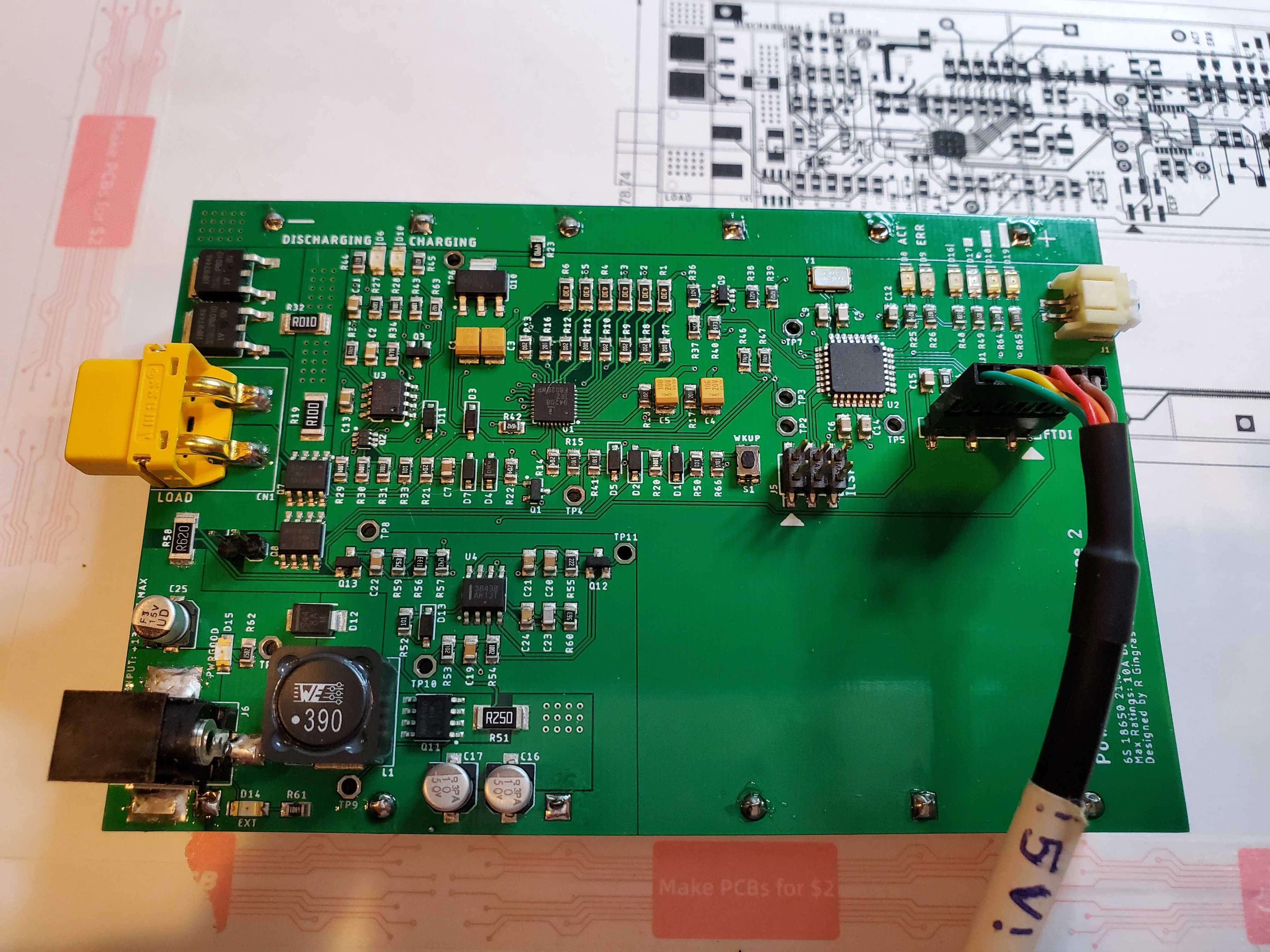
After completing and testing the Battery Bank Prototype 1, I was ready to move onto some of the next features I wanted to add. For the second prototype I focused on the switching boost converter charge circuit. I’ll briefly go over the design of that and how it relates to charging the battery pack.
Improvements/Fixes
- Added R63 to fix the charge indicator light always being on.
- Tightened up the reset line layout
- Added a button to wake the pack for programming
- Removed external charger header (was for testing anyways)
- Added a boost converter circuit for charging (see below)
Charging
Dave Jones at EEVBlog does an excellent job of explaining the basics of charging a Lithium-Ion battery:
What I designed was a simple switching boost converter that will deliver a maximum of 25.2V to the pack during charging, but also current limited to 1A. Once the charge current dips under 1A, the supply goes from constant-current to constant-voltage. Once charge current then drops below 100mA, the pack will stop the charging and go to sleep, thereby ending the charge cycle safely.
Boost Converter Design
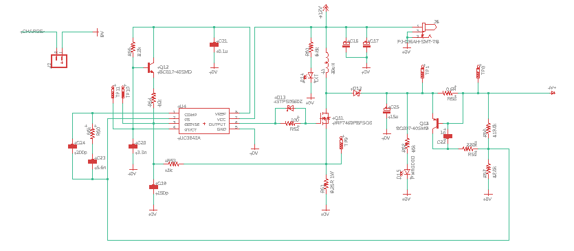
I created a simple worksheet to carry out all the calculations for the boost converter, which can be viewed here. I chose to go with a UC3843 Current-Mode SMPS Controller:

Current limiting is accomplished by Q13, R58 and R59. When the voltage drop across R58 gets large enough, Q13 starts to turn on and tugs the feedback voltage up, in turn telling the controller to reduce the voltage. R59 sets the gain of the current limiter. The initial value I chose of 75k ended up being to aggressive and pulled the voltage too high. After increasing it to 220k it now seems more stable, however due to excessive noise on the output I think it is causing the current limit to trigger early, reducing charge current to about 60% of target value (1A).
My plan to correct this is to adjust the design to reduce the voltage ripple (down to about 0.3% or 80mV) by adding more capacitance and reducing ESR. Going from 15uF to 44uF and reducing ESR from ~75mOhm to ~15mOhm should help.
Next Steps
On some advice I will be making a couple adjustments to the current regulation loop (mainly adding a base protection resistor), as well as addressing the excessive noise on the boost converter output by increasing capacitance and lowering ESR. I also am adding some decoupling in some spots.
For the next version I would like to replace the binary charge and discharge indicator circuits with actual current monitoring. For this I will set the dual op-amp up as two current sensing amplifiers (one inverting for charge sensing) and feed those outputs to two of the ADC inputs on the microcontroller. This accomplishes a couple goals: First, I can truly monitor the pack state of charge and do advanced capacity tracking. Second, I can make the charge and discharge cutoffs as high or low as I want without having to change out resistors.
There is another slight issue I’ve found with the board, and that is some small leakage current flowing through the charge circuit when the there is no power to it. I think the current (about 15mA) is finding its way through R41 and into the WKUP pin. Adding a diode between the CHARGE- terminal and R41 should prevent any current from flowing in that direction. Additionally, the WKUP pin is being pulled to almost full pack voltage which I think is interfering with proper operation of the WKUP circuitry. Removing the jumper that connects the charge circuit ground with pack ground solves the issue temporarily.
Resources
References
- Basic Calculation of a Boost Converter Power Stage (Texas Instruments)
- Maniktala. Switching Power Supply Design A-Z. Newness, 2015.
- Maniktala. Switching Power Supply Design and Optimization. McGraw-Hill, 2014.

Leave a Reply